
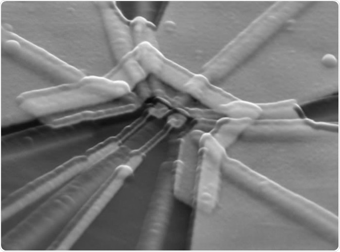
Electron beam Lithography is a specialized technology for creation of the extremely fine patterns that are required by the modern electronics industry for the integrated circuits. The technology works effectively due to the small spot size of the electrons. For the traditional optical lithography systems, the resolution is limited by the wavelength of light used for exposure.
How Does the Electron Beam Lithography Work?
The technique applied in electron beam lithography is derived from the early scanning of the electron microscopes. In brief, the electron lithography technique features scanning of the beam of electrons across a surface that is covered with a resist film, sensitive to the electrons. Therefore, the process deposits energy in the desired pattern on the resist film.
An Overview of How The Electron Beam Resists Are Processed?
Processing of the electron beam resists is straightforward. Ideally, the electron beam resists forms the recording and transfer media for E Beam lithography. The usual resists are the polymers dissolved in the liquid solvent. Therefore, the researchers drop the liquid resist onto the substrate and spin it at 1000 to 6000 revolutions per minute, forming a coating. After baking out the casting solvent, the electron exposure modifies the resist.
What Are the Parts of Electron Beam Lithography?
The electron beam lithography machine features three parts. The three parts are the electron gun, the vacuum system, and the control system. Therefore, the electrons are emitted from the filament tip and attracted to the anode. The emitted electrons are then focused into a beam using electromagnetic lenses. The electromagnetic lenses define the diameter of the spot size of the beam. The electromagnetic plates are used for correcting the astigmatism that might occur while focusing the beam.
Electron Beam Resists
The EBL resists are classified into two forms, just. These are the positive tone and the negative tone. Note that the legacy optical lithography systems also feature two resists. The positive resist develops away at exposed regions, while for the negative resist. The developed region remains after development.
A good example of the positive electron beam resist is the polymethyl methacrylate, which is the standard positive e-beam resist, and it is usually purchased in two high molecular weight forms.
Where is Electron Beam Lithography Useful?
e-Beam Lithography can be used in a wide range of application areas. The wide range of application areas includes semiconductor/superconductor interfaces in transportation studies. Other application areas include microsystem techniques and optical devices.
How Does Electron Beam Lithography Work compared to Other Methods?
Electron beam lithography represents a slow and expensive process. In fact, EBL is slower than photolithography, stamping, or the use of self-assembly methods for patterning. Bear in mind that the substrate charging and proximity error effects have to be taken into account to ensure good quality devices. Therefore, Electron Beam Lithography requires clean room facilities. The EBL is more suited for creating extremely high-resolution patterns or for creation of super unique items for which creation of photomask is time consuming or wasteful.
Overall, electron lithography offers a high patterning resolution compared to the lithography. The high patterning resolution is often because of the shorter wavelength possessed by the 10-50 keV electrons that it employs.
Parts of the Electron Beam Lithography System.
The EBL system comprises various parts. The parts include:
- The electron gun or the electron source supplying electrons
- An electron column that shapes and focuses the electron beam
- The mechanical stage used for positioning the wafer under the electron beam
- The water handling system for feeding wafers to the system automatically and unloading the wafers after processing
- Computer system that controls the other components
Similar to optical lithography, the electron lithography uses the positive and the negative resists often referred to as the electron beam resists. The E-beam resists are beam sensitive materials used for covering the wafers as per the defined pattern.
Electron Beam Lithography Industrial applications
The electron beam lithography is used in a wide range of areas. These include
- Cryo-electric devices
- Opto-electronic devices
- Quantum structures
- Transport mechanism studies
- Semiconductor / superconductor interfaces
- Microsystem techniques
- Optical devices
Conclusion
Lithography is subdivided into different types. Electron beam lithography is just one form of lithography. With electron beam lithography, a focused beam is scanned across the wafer, and the scan is done line by line.


Comments